Lith Corporation, founded in 1998 by a group of material science doctor from Tsinghua University, has now become the leading manufacturer of battery lab&production equipment. Lith Corporation have production factories in shenzhen and xiamen of China.This allows for the possibility of providing high quality and low-cost precision machines for lab&production equipment,including: roller press, film coater,mixer, high-temperature furnace, glove box,and complete set of equipment for research of rechargeable battery materials. Simple to operate, low cost and commitment to our customers is our priority.
DC Sputtering: Overview, Features, Process, Applications, Advantages, and Conclusion
DC Sputtering is a widely used thin-film deposition technique within the Physical Vapor Deposition (PVD) family, specifically designed for depositing conductive materials. It is a fundamental technology in both research and industrial environments, enabling precise, uniform, and adherent thin films on a variety of substrates. DC sputtering has become an essential tool in semiconductor fabrication, surface engineering, optics, and materials science due to its reliability, high deposition rates, and compatibility with a wide range of metallic targets.
Overview
DC Sputtering operates by applying a direct current (DC) voltage between a cathode (the target material) and the anode (typically the chamber or substrate holder) in a vacuum environment. An inert working gas, usually argon, is ionized under the applied voltage to form plasma. Positive ions from the plasma accelerate towards the target, dislodging atoms through momentum transfer. These ejected atoms then condense on the substrate, forming a dense and uniform thin film. Unlike other deposition methods such as thermal evaporation, DC sputtering allows for excellent adhesion, precise thickness control, and the deposition of complex multilayer structures.
Key Features of DC Sputtering Systems
Modern DC sputtering systems are designed for efficiency, precision, and reproducibility. Key features include:
High-Vacuum Chamber: Minimizes contamination and ensures high-purity film formation.
DC Power Supply: Provides stable voltage and current to maintain consistent plasma generation.
Magnetron Cathodes: Enhance plasma density near the target, improving deposition rate and target utilization.
Substrate Manipulation: Rotation, tilting, or biasing mechanisms ensure uniform coatings across complex geometries.
Process Monitoring: Integration of quartz crystal microbalances (QCM), pressure gauges, and automated control software for real-time deposition monitoring.
These features allow DC sputtering systems to produce high-quality coatings suitable for industrial and laboratory applications.
DC Sputtering Process
The DC sputtering process begins with evacuating the deposition chamber to achieve a high vacuum, by the introduction of argon gas. When DC voltage is applied, the argon atoms are ionized, forming a plasma. The positively charged argon ions accelerate toward the negatively biased target, knocking off target atoms. These atoms travel through the vacuum and condense onto the substrate, forming a uniform thin film.
DC sputtering is most effective for conductive targets such as metals (e.g., gold, copper, aluminum, or platinum). Variations of the process can include:
Reactive DC Sputtering: Introduction of reactive gases like oxygen or nitrogen to produce compound films such as oxides or nitrides.
Magnetron-Enhanced DC Sputtering: Employs magnetic fields to confine electrons near the target, increasing plasma density and deposition efficiency.
Multi-Target DC Sputtering: Allows co-deposition of multiple materials for alloy or multilayer film fabrication.
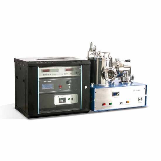
Magnetron Ion Sputtering Coater
Applications
DC sputtering finds extensive applications across multiple industries:
Microelectronics & Semiconductors: Deposition of conductive interconnects, electrodes, barrier layers, and contact pads.
Optics & Photonics: Coating of mirrors, anti-reflective layers, and optical filters.
Surface Engineering: Hard coatings, wear-resistant and decorative layers for metals, plastics, and ceramics.
Energy Devices: Fabrication of thin-film solar cells, transparent conductive oxides, and battery electrodes.
Materials Research: Development of nanostructured films, multilayer coatings, and customized thin-film compositions.
Advantages
DC sputtering offers several significant advantages:
High Deposition Rate: Efficient for conductive materials, enabling faster production cycles.
Excellent Film Adhesion: Produces dense, uniform coatings with strong substrate bonding.
Material Versatility: Compatible with metals, alloys, and some conductive compounds.
Reproducibility and Control: Automated monitoring ensures consistent film thickness and properties.
Low Substrate Heating: Suitable for temperature-sensitive substrates, including polymers and thin electronics.
Conclusion
In conclusion, DC Sputtering is a reliable, versatile, and high-performance thin-film deposition technique, particularly suited for conductive materials. Its ability to produce uniform, dense, and adherent coatings with precise thickness control makes it indispensable in microelectronics, optics, surface engineering, and energy device fabrication. By combining high deposition efficiency, reproducibility, and flexibility, DC sputtering continues to be a cornerstone technology in both research and industrial applications, enabling advancements in modern material science and surface engineering.


 +86 13174506016
 Louis@lithmachine.com
 +86 18559646958
 18659217588
 English ▼


