Lith Corporation, founded in 1998 by a group of material science doctor from Tsinghua University, has now become the leading manufacturer of battery lab&production equipment. Lith Corporation have production factories in shenzhen and xiamen of China.This allows for the possibility of providing high quality and low-cost precision machines for lab&production equipment,including: roller press, film coater,mixer, high-temperature furnace, glove box,and complete set of equipment for research of rechargeable battery materials. Simple to operate, low cost and commitment to our customers is our priority.
Sputter Coater: Overview, Features, Process, Applications, Advantages, and Conclusion
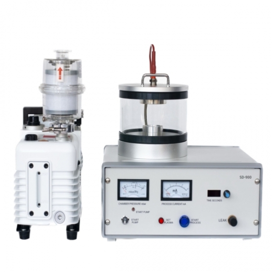
A Sputter Coater is a precision laboratory and industrial instrument used to deposit thin, conductive, or protective films onto various substrates through the process of physical vapor deposition (PVD). By utilizing a plasma-assisted sputtering mechanism, sputter coaters create uniform coatings that are critical for enhancing the surface properties of materials, such as electrical conductivity, adhesion, corrosion resistance, and imaging quality. This equipment is widely employed in research laboratories, electronics manufacturing, materials science, and microscopy sample preparation, particularly for scanning electron microscopy (SEM) and atomic force microscopy (AFM) applications.
Overview
The sputter coater operates by bombarding a solid target material with high-energy ions, typically generated in an inert gas plasma. This process ejects atoms from the target, which then condense onto the substrate to form a thin, uniform film. Modern sputter coaters are designed for precision, repeatability, and ease of use, often incorporating vacuum chambers, advanced power supplies, and automated control systems to ensure consistent deposition.
Unlike traditional evaporation techniques, sputter coating allows for the deposition of a wide range of materials, including metals, alloys, and some insulating compounds, while maintaining strong adhesion to the substrate and minimal substrate heating. This versatility makes the sputter coater a fundamental tool in both laboratory-scale experiments and industrial thin-film fabrication.
Key Features of a Sputter Coater
A high-quality sputter coater is characterized by several important features:
Vacuum Chamber Design: Ensures ultra-high vacuum conditions that minimize contamination and enable precise film growth.
Magnetron or Planar Targets: Enhance plasma density for efficient sputtering while reducing thermal load on the substrate.
Multiple Power Modes: DC, RF, and pulsed-DC options allow deposition of conductive and insulating materials.
Automated Substrate Rotation: Guarantees uniform film thickness and surface coverage, particularly for complex geometries.
Process Monitoring and Control: Integrated sensors and software provide real-time control of deposition rate, film thickness, and gas flow.
These features collectively ensure that the sputter coater delivers reliable, repeatable, and high-quality thin films suitable for a variety of applications.
Sputtering Process
The sputter coating process begins with evacuating the chamber to a high vacuum, by the introduction of an inert working gas such as argon. When voltage is applied to the target, a plasma forms in front of the target surface. Positive ions from the plasma are accelerated towards the target, dislodging atoms from the material via momentum transfer.
The ejected atoms then travel through the vacuum and deposit onto the substrate to form a thin, uniform coating. Variations in the sputtering process include:
DC Sputtering: Ideal for conductive materials such as gold, platinum, or copper.
RF Sputtering: Suitable for insulating or ceramic materials.
Reactive Sputtering: Combines reactive gases like oxygen or nitrogen with the target material to form compound films such as oxides or nitrides.
Co-Sputtering: Simultaneous use of multiple targets to create alloy or composite films with customized properties.
Lab Ion Sputtering Coater
Applications
Sputter coaters are widely used across research, industrial, and analytical domains:
Microscopy: Provides conductive coatings for non-conductive samples in SEM and AFM, reducing charging effects and improving image resolution.
Electronics: Deposits thin conductive and protective layers on circuit boards, sensors, and microelectronic devices.
Materials Science: Enables the fabrication of multilayer films, alloy coatings, and nanostructured materials for research purposes.
Surface Engineering: Produces corrosion-resistant, wear-resistant, and decorative coatings on metals, plastics, and ceramics.
Advantages
The advantages of using a sputter coater include:
Uniform and High-Quality Coatings: Produces dense, smooth films with strong adhesion to substrates.
Material Versatility: Can deposit metals, alloys, and some insulating compounds.
Low Substrate Heating: Protects temperature-sensitive materials and allows coating of polymers and delicate electronics.
Reproducibility and Control: Automated processes and real-time monitoring ensure consistent film thickness and composition.
Minimal Contamination: High-vacuum operation reduces oxidation and other impurities during deposition.
Conclusion
In summary, the Sputter Coater is a versatile and essential instrument for thin-film deposition in research, industrial, and analytical applications. Its combination of precise process control, uniform coating capabilities, and material flexibility makes it an invaluable tool for microscopy sample preparation, electronics fabrication, and surface engineering. By enabling the deposition of high-quality, reproducible thin films with minimal substrate damage, sputter coaters continue to play a critical role in advancing material science, electronics, and nanotechnology.


 +86 13174506016
 Louis@lithmachine.com
 +86 18559646958
 18659217588
 English ▼


