Lith Corporation, founded in 1998 by a group of material science doctor from Tsinghua University, has now become the leading manufacturer of battery lab&production equipment. Lith Corporation have production factories in shenzhen and xiamen of China.This allows for the possibility of providing high quality and low-cost precision machines for lab&production equipment,including: roller press, film coater,mixer, high-temperature furnace, glove box,and complete set of equipment for research of rechargeable battery materials. Simple to operate, low cost and commitment to our customers is our priority.
Sputtering System: Overview, Features, Processes, Applications, and Advantages
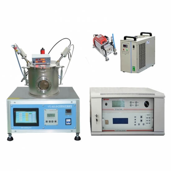
A Sputtering System is a core piece of vacuum deposition equipment widely used in the manufacturing of thin films and functional coatings. As one of the most mature and controllable Physical Vapor Deposition (PVD) methods, sputtering enables the precise transfer of atoms from a solid target to a substrate through high-energy ion bombardment. This technique is essential for industries such as semiconductors, optics, energy storage, surface engineering, and advanced electronics, where film uniformity, adhesion, and reproducibility are critical. Modern sputtering systems integrate sophisticated plasma control, vacuum engineering, and automated handling to achieve high-quality thin-film deposition tailored to industrial or research requirements.
Key Features of a Sputtering System
A typical sputtering system is designed to deliver stable and repeatable deposition performance through a combination of hardware precision and advanced control electronics.
Vacuum architecture is one of its core features, usually involving a multi-stage pumping configuration comprising rotary pumps, turbomolecular pumps, and sometimes cryogenic pumps. This ensures extremely low base pressures, which are necessary to reduce contamination and enable consistent film growth.
Another defining feature is the sputtering cathode or magnetron source, which generates a dense plasma environment that facilitates high sputtering rates and excellent ionization efficiency. Magnetron sputtering systems utilize magnetic fields to trap electrons near the target surface, improving energy transfer and minimizing substrate heating—an essential requirement for temperature-sensitive materials.
Modern sputtering systems are also equipped with real-time monitoring and automated control functions, including mass-flow controllers, power supplies with DC, RF, or pulsed-DC modes, substrate temperature modules, and optional in-situ film characterization tools such as quartz crystal microbalance (QCM). These features ensure that film thickness, rate, and composition remain within tight tolerances.
Sputtering Processes and Working Principles
The operation of a sputtering system relies on plasma-assisted material transfer. During operation, a controlled atmosphere—typically argon—is introduced into the vacuum chamber. A high voltage applied to the target cathode ionizes the gas, creating positively charged ions that are accelerated toward the target surface.
Upon impact, these ions eject atoms from the target through momentum transfer. These atoms then travel across the low-pressure environment and condense onto the substrate to form a thin film. The process can be refined or adapted depending on the deposition requirements:
DC Sputtering: Ideal for conductive metal targets and offers stable, high-rate deposition.
RF Sputtering: Used for insulating or ceramic targets by preventing charge buildup on the target surface.
Magnetron Sputtering: Enhances plasma density and deposition efficiency, reducing substrate heating.
Reactive Sputtering: Introduces reactive gases such as oxygen or nitrogen to form compound films (e.g., oxides, nitrides).
Co-Sputtering: Uses multiple targets to create customized alloy or multi-component films with tunable composition.
Each process configuration plays a crucial role in defining the film’s microstructure, purity, and performance characteristics.
Magnetron Sputtering System
Applications of Sputtering Systems
Sputtering systems are indispensable in high-technology industries where precision coatings are required. In the semiconductor field, sputtering is used to deposit diffusion barriers, interconnect metals, dielectric layers, and gate materials. Its reliability and uniformity make it compatible with integrated circuit fabrication and wafer-level packaging.
In optics, sputtering systems are used to create anti-reflective coatings, dielectric mirrors, optical filters, and protective layers for lenses. The high uniformity of magnetron sputtering is particularly beneficial for large-area optical components.
The energy sector also relies heavily on sputtering systems. Thin-film solar cells, battery electrodes, and transparent conductive oxides (TCOs) can be deposited with excellent adhesion and stability. For example, indium tin oxide (ITO) and nickel oxide films are commonly prepared using reactive sputtering.
In surface engineering, sputtering is used to produce hard coatings, wear-resistant layers, decorative finishes, and corrosion-resistant surfaces on metals, plastics, and ceramics. Industries such as automotive, aerospace, and tooling benefit significantly from these advanced coatings.
Advantages of Sputtering Systems
Sputtering systems provide several substantial advantages over other thin-film deposition techniques. One major advantage is excellent film uniformity and adhesion, resulting from the energetic nature of sputtered atoms. This leads to dense, smooth coatings with strong bonding to the substrate.
Another important advantage is the ability to deposit a wide range of materials, including metals, semiconductors, insulators, and complex compounds. With reactive and RF sputtering, even materials that are difficult to evaporate can be deposited accurately.
Sputtering also ensures high reproducibility and control, as parameters such as power, pressure, gas flow, and substrate temperature can be finely tuned. This makes it suitable for mass production as well as laboratory-level research.
Finally, sputtering operates at relatively low substrate temperatures, enabling coating on polymers, flexible substrates, and temperature-sensitive electronics.


 +86 13174506016
 Louis@lithmachine.com
 +86 18559646958
 18659217588
 English ▼


